
Testing of printed circuit boards (PCBs) is a critical step in the process of manufacturing electronic devices. This stage is essential to ensure the quality and reliability of the products. We use a wide range of test
methods, including visual inspection, AOI (Automated Optical Inspection), functional testing and X-ray inspection, to ensure that each product meets the highest standards.
Our processes are designed to detect and correct any defect, minimizing the risk of errors and increasing overall product reliability.
1. Visual inspection:
The first step is a visual inspection, where the technician inspects the PCB visually for defects such as missing components, incorrect mounting, missing or damaged connections, and other visible problems.
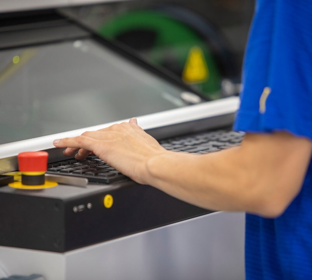
2. Automated Optical Inspection (AOI):
This method uses cameras and software to automatically inspect the PCB based on specified criteria, such as correct component placement, correct polarization, correct orientation, and quality of solder joints. We use AOI Cyber Optics for this inspection.
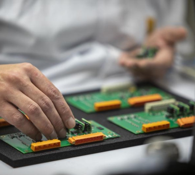
3. Functional testing:
This method involves verifying that the product is working properly. The PCB is connected to a test device that simulates real operating conditions and checks that all functions of the device are working as intended.
4. X-ray inspection:
X-ray inspection allows you to view the internal structure of the PCB, making it easy to detect defects and errors such as missing components, faulty connections, short circuits, and other problems that could lead to malfunctioning or unreliable electronic devices.
The combination of these methods will provide us with the most reliable and high-quality result. Testing of assembled printed circuits is crucial for quality assurance in electronic manufacturing.


Each component used in the assembly of a printed circuit board had a unique identification number. This number is recorded in the ERP database and is assigned to a specific printed circuit board.
Each step in the PCB assembly process is recorded and assigned to a specific product. This includes information about when the component was fitted, who fitted it, what device was used.
Information about testing and quality control processes is also part of traceability. This makes it possible to identify products with defects and track how these defects have been repaired.
If a problem with a printed circuit board occurs later, traceability allows it to be tracked. This means that you can identify all printed circuits that have been manufactured using the same components or processes and take the necessary steps to improve quality.
In some industries, such as healthcare or aviation, strict standards and regulations regarding traceability are required. This is to ensure the safety and quality of the products.
Overall, traceability in PCB assembly helps to increase product quality, reduce the risk of errors, and makes it easier to track the manufacturing process from start to finish. We manage this traceability with software systems that allow for easy monitoring and management of data.
At the customer's request, we provide an FAI report during primary production. The First Article Inspection Report (FAIR) is a documentation process used in the electronics and printed circuit board (PCB) industries, especially in the production of electronic devices. This process aims to ensure that the first batch of products meets the customer's specifications and requirements, and that the production process is well set up.
FAIR typically involves the following steps:
1. Gaining documentation
2. Sampling
3. Product Inspection
4. Dealing with identified deficiencies
5. FAIR Report
6. Customer approval
FAIR is an important step in the quality assurance process of electronic components and devices. It helps identify and resolve issues in the early stages of production, which can significantly reduce the cost of corrections later in the manufacturing process. In addition, FAIR helps to ensure that the products meet the customer's requirements and are safe and reliable.

Do you have questions, comments or are you just curious? We are here for you! Contact us through the channels below or using the form.