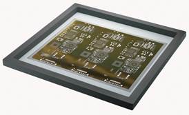
MARPOS is a Czech manufacturer of printed circuit boards (PCB). We offer whole product range of PCB from one-sided to twelve-layer including those with an aluminum base. We began PCB production in 2001. Our team of experienced workers offer you professional help by means of PCB design and production solutions. In our company minimum order quantity does not exist. You can order from one to a thousand pieces of PCB. We focus on high production efficiency, flexibility and minimised expenditure. We offer fast delivery, high quality and favorable prices. We are certified by the company TÜV SÜD Czech according to ČSN EN ISO 9001:2009 and ČSN EN ISO 14001:2005. Our team of experienced workers and modern technology offer production of the highest possible quality. Our company target is to manufacture products which are competitive with global competition. Our products are used widely in fields of telecommunications, CNC machines, the health sector, the automobile industry, energetics and other high-tech areas.
We offer to customers who are interested in low-cost production PCB carried out in China. We have been cooperating with leading Chinese manufacturers for many years. Production data is controlled and panellised by our technology worker. PCB made in China goes through the Chinese electronic test and our optical inspection
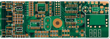
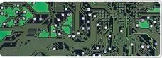
Printed circuit board (PCB) is a board of insulating material with copper electrical connections (tracks) and solder points which are intended for mounting electronic components. The connections on the boards are made by chemical etching baths and bias in the galvanic line. Printed circuit boards are monolayer, double-layer and multilayer (inner layer). Electronic components are placed on the board at the via holes (THT technology) or pads (surface SMT). In the first case, the electronic component PTO and soldered on the other side than it is placed. In the second case, the components are soldered to the side where they are located.


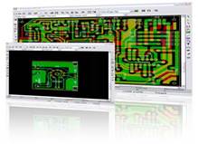
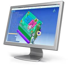
Printed circuit boards are designed in CAD prorammes (for example Altium, Eagle, Protel, OrCAD)

The proposed new product is a new type of industrial product it requires to be tested before the decision to manufacture it or before manufacture begins. Therefore, it must first start with the production of a functional prototype. This is understandably difficult as we do not yet have manufacturing tools of mass production and therefore must produce it more or less by hand and in a few pieces.
For that reason we offer to produce prototypes catering to the needs of developers, designers and students. To this end we manufacture PCB in small series. (NB it must be agreed with the technologist before production starts).
Terms of service PROTOTYPE :
Orders made on weekdays until 12:00 will be made the following day and be ready for delivery from 14:00. Next day production means production time, It doesn´t mean the postal delivery.If you need DPS very quickly it is necessary to pick it up in person.
The customer will be informed about the production date by e-mail or SMS.
The customer has the option to pick the finished product, or have it sent to them by post.
Next day production is only possible for single- and double-layer PCB. Multi-layer PCB and AL PCB require a minimum of 7 days to be manufactured.
Surcharges for express production:
|
24 hours |
3 days |
7 days |
|
|
monolayer PCB |
200% |
75% |
20% |
|
doublelayer PCB |
200% |
100% |
30% |
|
multilayer PCB |
not available |
not available |
200% |
|
Auminium PCB |
not available |
not available |
100% |
The most basic PCB have electronic components on one side and conductive paths (connections) on the other. Due to the fact that the conductor is only on one side, this PCB is called the unilateral or one-layer PCB. This type of board is only suitable for simple circuits because the connections are only one-sided. They cannot lead to a second; they may only lead around themselves.
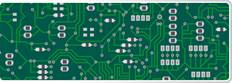
Double-layer (bilateral) PCB are more suitable for more demanding circuits as they have an area double the size for guiding connections (paths) as opposed to the single-layer printed circuit board. Bilayer boards have conductors on both sides and are connected by vias.
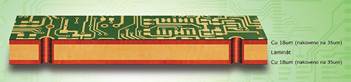
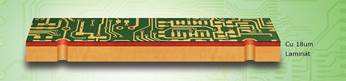
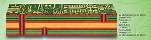
Multilayer PCBs have one or more internal conductive layers. This is achieved by compressing the core, coppered layers and insulating prepregs. The number of layers is referred to as the number of “themes”. The vias in multilayer boards are reversible and penetrate the whole board. Blind vias connect one of the outer layers with one or more of the internal layers. Where we want to combine only the inner layer we use the buried vias.
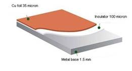
In electronics, which requires improved performance and increased heat dissipation, a material with metal core (metal core PCB) is used. Conventional materials such as FR4 and CEM1 cannot dissipate enough heat and nor does it have a sufficiently low coefficient of thermal expansion (CTE) which are needed to comply with the latest construction demands (BGA, LED lights). Instead of the classic base materials such as FR4 or CEM1 metal cores are used in the printed circuits: mostly aluminum or copper alloys. The main advantage of metal core PCB (MCPCB) is that it can efficiently dissipate heat from electronic components. This is achieved by a thermally conductive dielectric, acting as a thermal bridge between the components and the metal support plate.
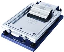
SMT templates are used for applying solder paste on PCB pads. Etching on the film with alpaca or phosphor-bronze creates openings for each component allowing surface mounting on the board. The template is then set by screen printing to motive of the board and solder paste is applied through the holes by use of wipers. Once the template tears off the board the solder paste stays ready to lay SMD components. This process, unlike the manual soldering, ensures consistency and saves time.
The film thickness and hole size gives us the volume of the paste deposited on the plate surface. Too much solder paste causes the board to short-circuit and decentralisation of components. Lack of solder paste causes a lack of soldered components. All these shortcomings cause poor electrical functioning of the board.
The correct thickness of the film is chosen based on the type of components mounted on the board. Size 0603 components need thinner foil and 1206 components thicker foil. The thicknesses of the film used for most of the plates is 100, 150 and 200 microns.
We produce templates for our own use and for that of external companies.